
Contact Us


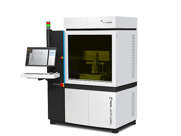
FINEPLACER® femto 2
Advanced Sub-Micron Bonder
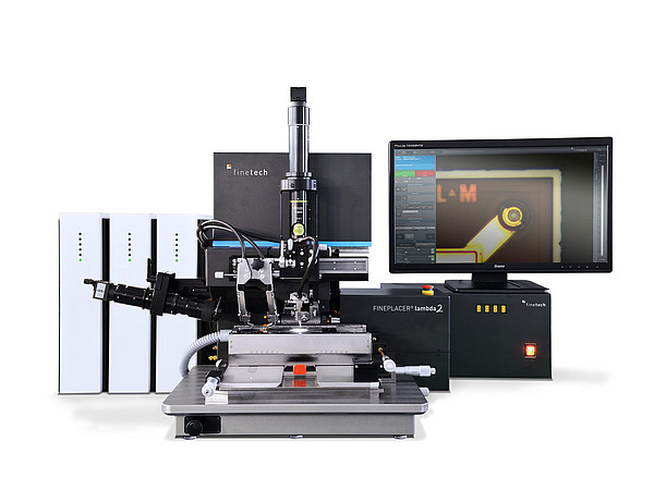
FINEPLACER® lambda 2
Sub-Micron Table Top Die Bonder
Advanced Sub-Micron Bonder
Sub-Micron Table Top Die Bonder