
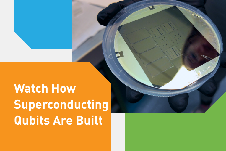
// Watch How Superconducting Qubits Get Built
See how superconducting qubits are flip-chip bonded for 3D integration at Peak Quantum and the Walther-Meißner-Institut (WMI). Our video shows why advanced packaging is key to scaling quantum computing.
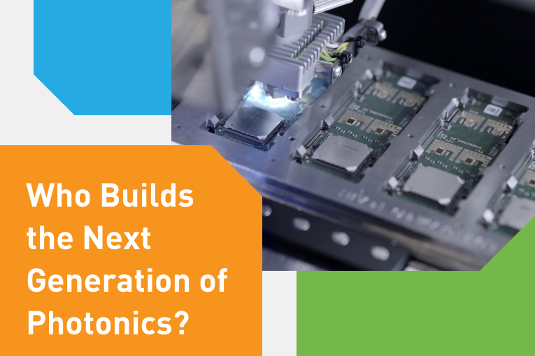
// Who Gets to Build the Next Generation of Photonics?
The best chip doesn’t decide who builds the next generation of photonics. The handoff from lab to volume does, the point where most advanced packaging quietly breaks. A look at
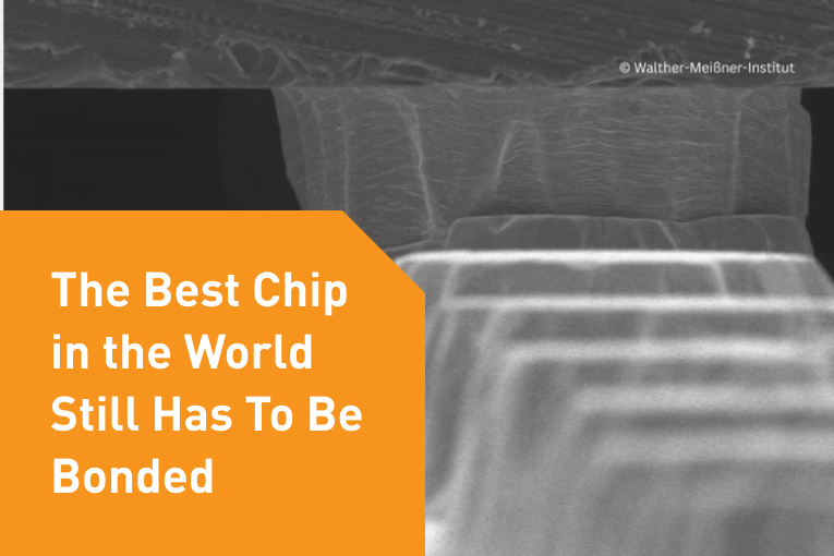
// The Best Chip in the World Still Has to Be Bonded
Indium bump interconnect has quietly become the step that makes or breaks IR sensors, quantum processors and microLED displays. This blog breaks down why this one flip-chip bond now decides
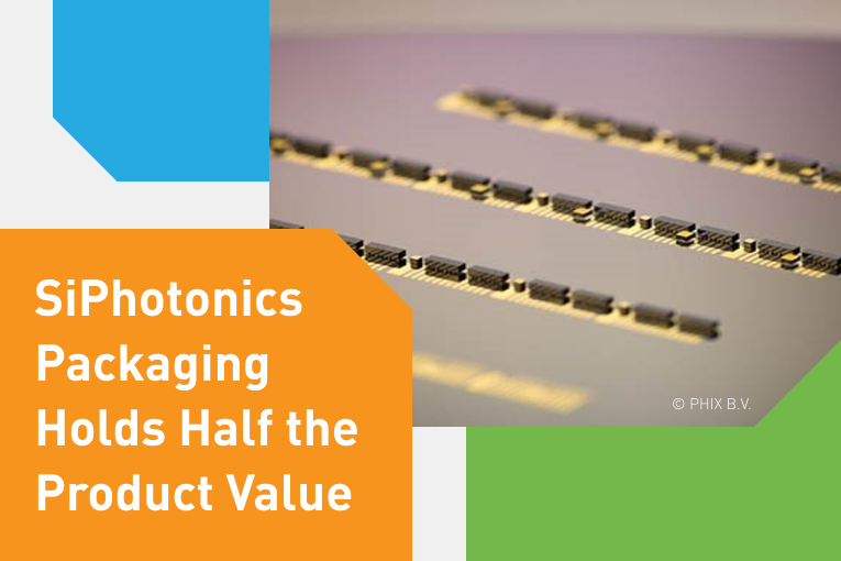
// Why Silicon Photonics Packaging Now Holds Half the Product Value
Silicon photonics packaging now carries up to half the product value. A perfect chip means nothing if the assembly around it fails. Where processes break on the way to production,
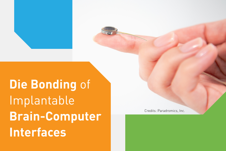
// How Implantable Brain-Computer Interfaces Are Pushing the Boundaries of Precision Die Bonding
Implantable BCIs are pushing the limits of precision die bonding and advanced packaging. Explore the assembly challenges behind this emerging technology and the processes needed to turn prototypes into reliable
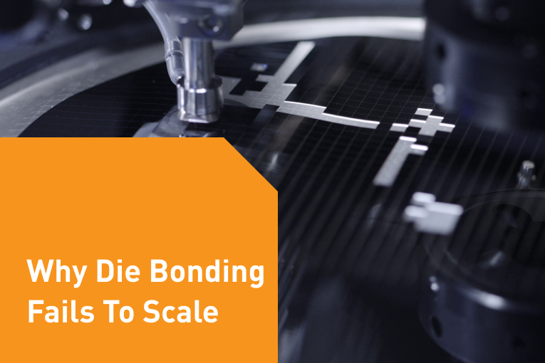
// Why Die Bonding Fails to Scale: How Do You Move from Prototype to Production Without Starting Over?
Avoid restarting development when scaling die bonding. Build stable, transferable processes early to reduce risk and achieve consistent yield from prototype to production.