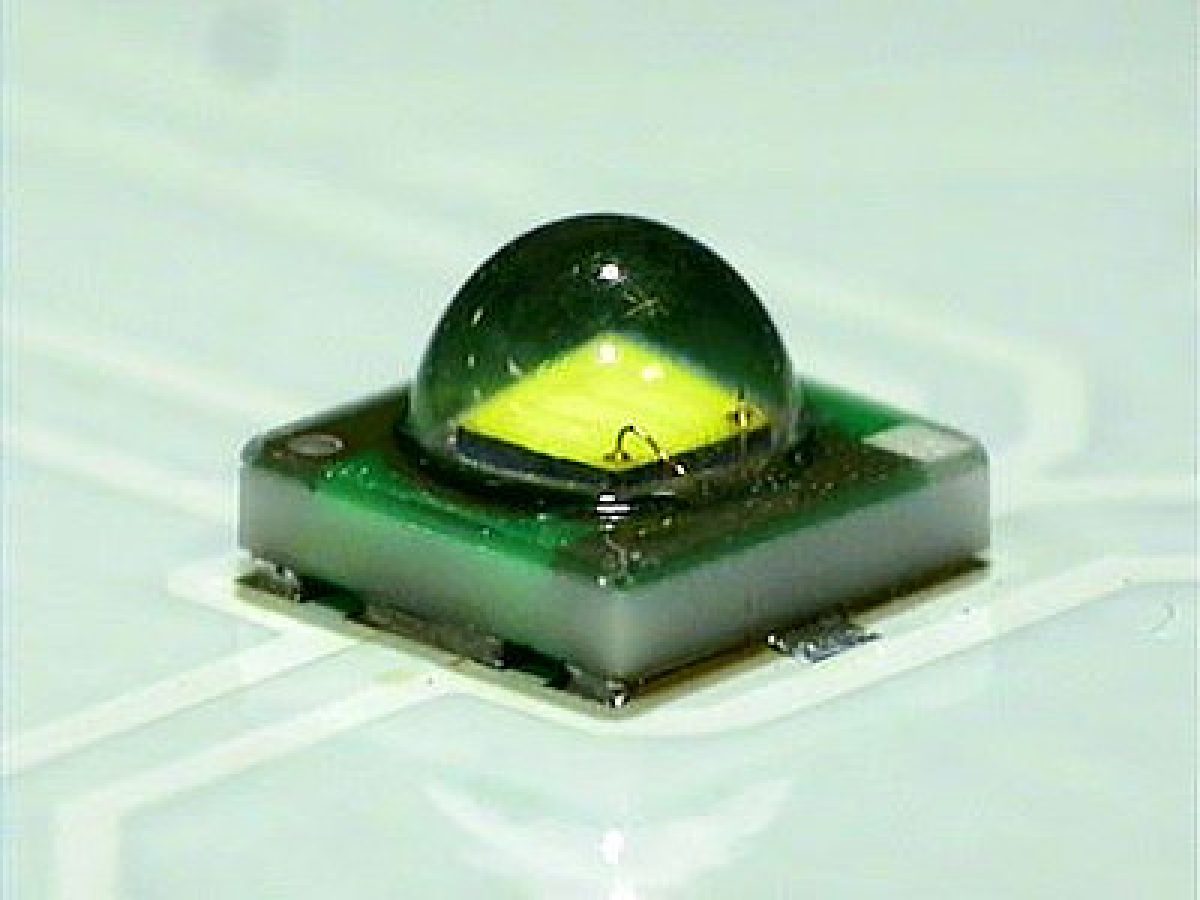
Light Emitting Diodes (LEDs) are by definition a two-lead semiconductor light source, which release energy in the form of photons that have the color of light. What color? Well, likely the most popular are Red, Green, Blue (RGB) and now White and other colors (Orange, as an example). Using different materials determines the color of an LED. For instance, Red, Orange and Yellow LEDs are made from Aluminum Gallium Indium Phosphide, whereas Green, Blue and White LEDs are made from Indium gallium Nitride.
In 2014 Dr. Shuji Nakamura was awarded the Nobel Prize for the invention of a White LED. Other colors had already been developed, but it’s been said that Nakamura’s LED success at the University of Santa Barbara was as noteworthy as Edison’s invention at the turn of the 20th century. Pretty significant.
Though LEDs produce more lumens (measured light) compared to incandescent lamps, halogen lamps, etc, there has long been a debate as to whether or not LEDs will be around long term. A big concern has been the environmental waste that results from LED manufacturing. Regardless of environmental concerns, LEDs appear to be here to stay. They are replacing incandescent type products and are used in nearly every market that requires light – from cell phones and smart watches to the illumination in a refrigerator or automobile.
So what are the advantages of LEDs versus incandescent or halogen bulbs? LEDs are so much more efficient than other light sources. Take for example Christmas lights. To illuminate a 500 foot string of C9 bulbs, it would require approximately 3,500 watts of power. Compare this to only 480 watts of power for LEDs — roughly 7x more efficient than the incandescent bulb.
As this industry evolves, Finetech equipment is playing a key role in the development and implementation of innovative LED technology. We work with companies large and small, from startups to Fortune 500s that are looking to capitalize on a market that seems to have very high potential. At the development level, Finetech systems may be involved in die bonding the first sample set from a wafer, or reworking µLEDs. Our ability to place and bond die as small as 0.03 x 0.03mm is unique, as well as our expertise in reworking individual pixels without disturbing neighboring LEDs. And we provide excellent thermal management and optical resolution, both critical factors when working with these devices.
Manual to automation…we have it covered! Check out how we helped an Asian display manufacturer improve its production yield for small SMD LED carrier boards.
07/04/2018, created by: Robert Avila

