// Watch How Superconducting Qubits Get Built
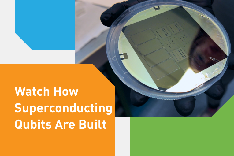
See how superconducting qubits are flip-chip bonded for 3D integration at Peak Quantum and the Walther-Meißner-Institut (WMI). Our video shows why advanced packaging is key to scaling quantum computing.
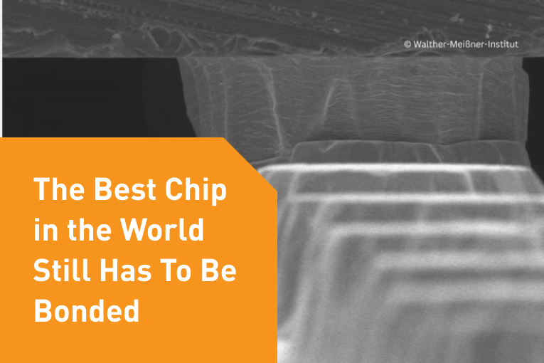
See how superconducting qubits are flip-chip bonded for 3D integration at Peak Quantum and the Walther-Meißner-Institut (WMI). Our video shows why advanced packaging is key to scaling quantum computing.
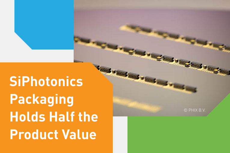
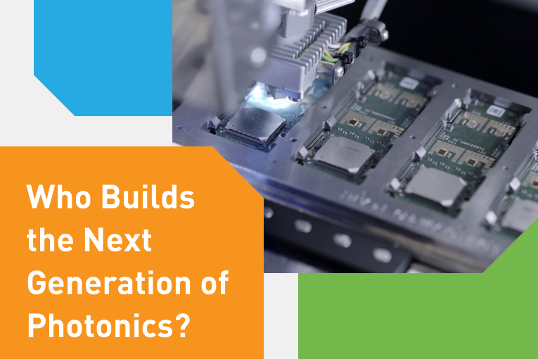
The best chip doesn’t decide who builds the next generation of photonics. The handoff from lab to volume does, the point where most advanced packaging quietly breaks. A look at what really decides that transfer, from the right accuracy to the handoff between development and production, and what it takes to carry a process from prototype to volume without starting over.

Indium bump interconnect has quietly become the step that makes or breaks IR sensors, quantum processors and microLED displays. This blog breaks down why this one flip-chip bond now decides whether a device reaches production, and what it takes to master indium bump interconnect at scale.

Silicon photonics packaging now carries up to half the product value. A perfect chip means nothing if the assembly around it fails. Where processes break on the way to production, and what it takes to scale.

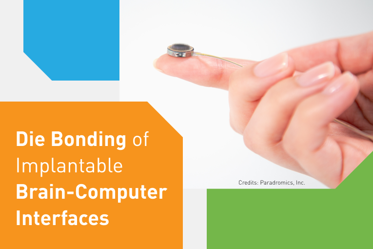
Implantable BCIs are pushing the limits of precision die bonding and advanced packaging. Explore the assembly challenges behind this emerging technology and the processes needed to turn prototypes into reliable medical devices.

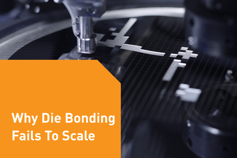
Avoid restarting development when scaling die bonding. Build stable, transferable processes early to reduce risk and achieve consistent yield from prototype to production.
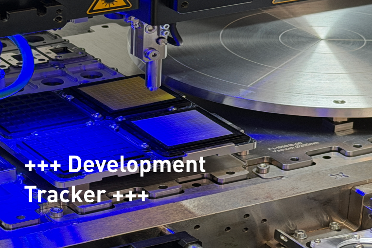
Follow the ongoing development of our next-generation production die bonder for high-mix manufacturing. This tracker collects the latest updates, engineering milestones, and insights as the platform advances with 12-inch readiness to support advanced semiconductor, photonic, and heterogeneous integration assemblies at scale.

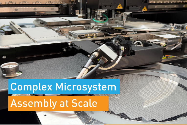
As advanced packaging moves toward wafer level and higher integration density, production stability is becoming a defining capability for manufacturers scaling complex assemblies beyond R&D into reliable volume production.

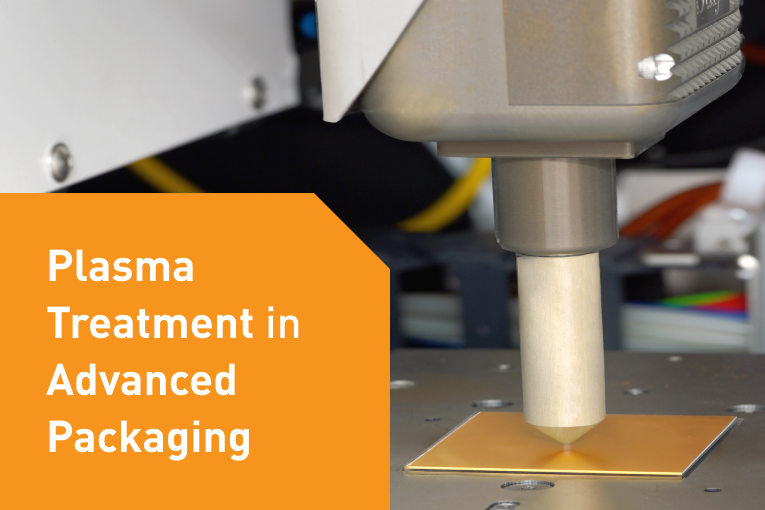
Bond quality is decided before bonding even begins. In advanced packaging, surface condition often limits yield and reliability more than placement accuracy. Plasma treatment prepares clean, stable interfaces immediately before bonding, reducing variability and improving bonding reliability.

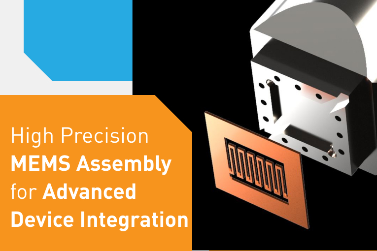
As MEMS devices are increasingly integrated with ASICs, optics and other components, assembly becomes a defining factor for performance, yield and reliability. This article explores current trends and requirements in MEMS assembly for advanced device integration.