Author: Dr. Carlo Pagano
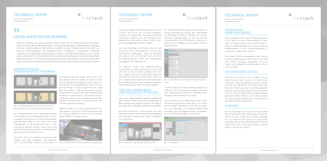
Abstract: Finetech’s laser-assisted die bonding technology is suitable for C2S and C2W applications with highest requirements regarding process speed, accuracy and precisely controlled local heat input even to smallest areas. Particularly quick temperature cycles minimize the risk of surface oxidation and allow shorter process cycles in time-optimized production environments. During sequential substrate-level or wafer-level bonding processes, each chip will be heated up only once. As opposed to area heating, localized laser heating does not require extensive provisions to avoid thermal expansion. Chips can be bonded with an edge-to-edge clearance of only 500 micron, with adjacent solder dots being reliably protected from (re-)melting.
Depending on the application and materials, two technologies are supported. If the chip/substrate is transparent to the wavelength of the light (e.g. fused silica, sapphire, etc.), the laser’s energy passes through without significant absorption effects and is used to heat the solder directly. With non-transparent substrate materials (Si, Ply-Si, GaAs, etc.), the laser’s energy is absorbed and converted into a local heat source used for the bonding process.


